

Difference Between NPN and PNP Transistor with Operation
Find the difference between NPN and PNP transistor below. The choice between NPN and PNP transistors depends on the specific requirements of a given electronic circuit. Both types have their advantages and applications.
Difference Between NPN and PNP Transistor: A transistor, specifically a bipolar junction transistor (BJT), is a semiconductor device featuring three terminals, three layers, and two junctions. Its primary functions within electronic circuits include serving as a digital switch and amplifier.
The transistor is constructed with three layers of semiconductor materials, namely P-type and N-type, organized into the emitter, base, and collector. Each layer contributes to the transistor's operation; the three terminals are derived from these layers. There are two main types of transistors based on the arrangement of these semiconductor layers. NPN transistor and PNP transistor. This article delves into the intricacies of NPN transistors (BJTs) and PNP transistors, exploring their structures, functions, and the critical distinctions between the two| NEET Physics Syllabus | NEET Physics Important Questions with Answers |
| NEET Physics Chapter wise Weightage | NEET Physics MCQs |
| NEET Physics Notes | NEET Physics Formulas |
Difference Between NPN and PNP Transistor Overview
The transistor, a crucial semiconductor device in electronic circuits, transfers or exchanges small signals within the circuit. It plays a pivotal role in regulating, processing, or amplifying signals like voltage or current, providing control over the flow within the circuit. The transistor's ability to manage current flow has classified transistors into two main types: NPN (Negative-Positive-Negative) and PNP (Positive-Negative-Positive). One significant difference between NPN and PNP transistors lies in the direction of current flow. NPN transistors utilize electrons as the majority carriers, while PNP transistors rely on holes as the majority carriers. This fundamental contrast in the charge carriers distinguishes the operation and characteristics of these transistors. In the upcoming sections, this article aims to provide readers with a concise yet comprehensive understanding of both NPN and PNP transistors, shedding light on their unique properties and applications.Difference Between NPN and PNP Transistor
NPN transistors are widely used for signal amplification in electronic circuits. They can amplify weak signals and are essential in audio amplifiers, radio frequency amplifiers, and other signal-processing applications. PNP transistors are also widely used for signal amplification in electronic circuits. They also play a crucial role in applications where amplifying signals is essential, such as in audio amplifiers, radio frequency circuits, and communication systems. Below table shows the difference between NPN and PNP transistor :|
Difference Between NPN and PNP Transistor |
|||
|---|---|---|---|
| Sr. No. | Criteria | NPN Transistor | PNP Transistor |
| 1 | Type of Semiconductor | N-type (Negative) | P-type (Positive) |
| 2 | Polarity | Current flows from collector to emitter. | Current flows from emitter to collector. |
| 3 | Majority Charge Carriers | Electrons (Negative charge carriers). | Holes (Positive charge carriers). |
| 4 | Operation | Current is carried by electrons. | Current is carried by holes. |
| 5 | Voltage Configuration | Collector is more positive than the emitter. | Emitter is more positive than the collector. |
| 6 | Switching Applications | Commonly used in low-side switching. | Commonly used in high-side switching. |
| 7 | Voltage Biasing | Requires a positive voltage bias. | Requires a negative voltage bias. |
| 8 | Applications | Commonly used in amplifiers and low-side switching applications. | Commonly used in amplifiers and high-side switching applications. |
| 9 | Notation | NPN: Not Pointing iN (arrow points outward from the base). | PNP: Pointing iN P (arrow points inward toward the base). |
| 10 | Symbol Convention | Arrow points away from the base. | Arrow points toward the base. |
| 11 | Full Form | Negative-Positive-Negative | Positive-Negative-Positive |
| 12 | Invention Year | Introduced earlier in the history of transistors. | Introduced later than NPN transistors. |
What is NPN Transistor?
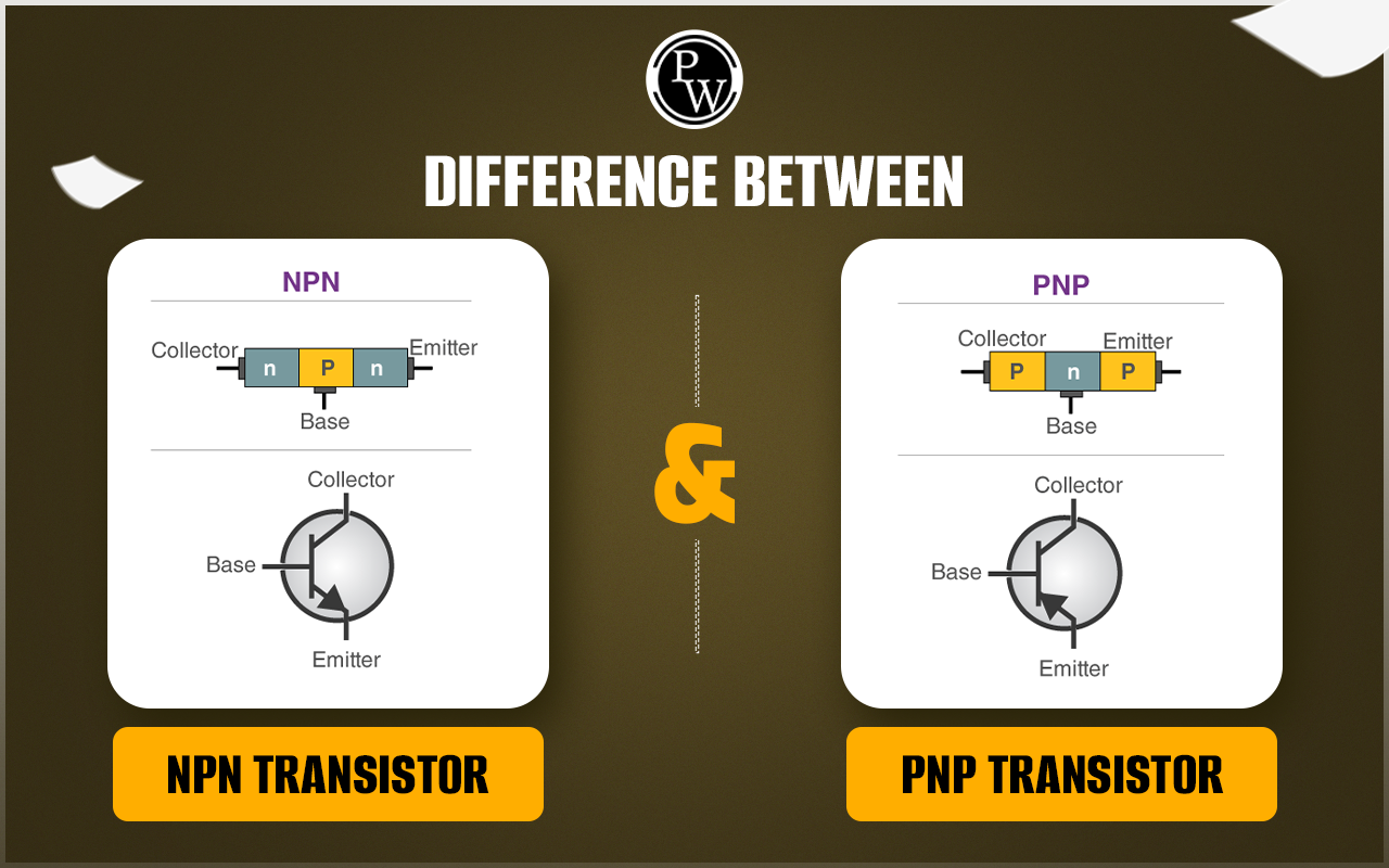
The NPN transistor stands as one of the most commonly used bipolar junction transistors. Its construction involves placing a semiconductor of the P-type between two semiconductors of the N-type. The NPN transistor comprises three terminals – collector, emitter, and base. Functionally, the NPN transistor operates like two PN junction diodes connected in reverse, also known as the collector-base junction or base-emitter junction.Operation of the NPN transistor
The operation of the NPN transistor involves the following steps:- A small voltage between the base and emitter propels electrons from the N-type emitter to the P-type base.
- Some electrons traverse the base and enter the N-type collector region.
- A voltage between the emitter and collector attracts the electrons into the collector, creating a collector current regulated by the base current.
- The transistor amplifies by transforming the small base current into a larger collector current.
- The base current dictates whether the transistor is off (cutoff), on (saturation), or in an intermediate state (active region).
- The transistor amplifies or switches signals by controlling the collector current with the base current.
What is PNP Transistor?
The PNP transistor belongs to the category of bipolar junction transistors, and it is constructed using a sandwiching technique that places the N-type semiconductor between two P-type semiconductors. This transistor comprises three terminals: collector, emitter, and base. Functionally, the PNP transistor operates like two diodes for PN junctions connected back-to-back, commonly known as the collector-base junction or base-emitter junction.Three terminals of the PNP transistor
- Emitter: This region provides charging carriers to the collector, and the emitter sends charge carriers to the collector through the base region.
- Collector: This region collects the majority of charge carriers released by the emitter.
- Base: This region triggers and regulates the amount of current flowing from the emitter to the collector. The accompanying image illustrates the symbol and structure of the PNP transistor.
Operation of the PNP transistor
The operation of the PNP transistor involves the following steps:- A small negative voltage between the base and emitter propels holes from the P-type emitter into the N-type base.
- Some holes traverse the base and enter the P-type collector region.
- A voltage between the emitter and collector attracts the holes into the collector, creating a collector current controlled by the base current.
- The transistor amplifies by transforming the small base current into a larger collector current.
- The base current dictates whether the transistor is off (cutoff), on (saturation), or in an intermediate state (active region).
- The transistor serves to amplify or switch signals by controlling the collector current with the base current.
Difference Between NPN and PNP Transistor FAQs
Which transistor is considered "electron flow" and which one is considered "hole flow"?
In an NPN transistor, current flow is due to the movement of electrons (electron flow). In a PNP transistor, current flow is considered due to the movement of holes (hole flow).
How is the current direction defined in an NPN transistor?
In an NPN transistor, current flows from the collector (C) to the emitter (E), and the arrow in the symbol points in the direction of conventional current flow.
How is the current direction defined in a PNP transistor?
In a PNP transistor, current flows from the emitter to the collector, and the arrow in the symbol points in the direction of conventional current flow.
Which type of transistor is more common in electronic circuits?
NPN transistors are more commonly used in electronic circuits due to their ease of implementation and higher electron mobility.
How does the biasing arrangement differ in NPN and PNP transistors?
The biasing arrangement is the opposite. In an NPN transistor, the base-emitter junction is forward-biased, while in a PNP transistor, it is reverse-biased.


🔥 Trending Blogs
Talk to a counsellorHave doubts? Our support team will be happy to assist you!

Check out these Related Articles


Join 15 Million students on the app today!

Free Learning Resources
PW Books
Notes (Class 10-12)
PW Study Materials
Notes (Class 6-9)
Ncert Solutions
Govt Exams
Our Other Websites
Class 6th to 12th Online Courses
Govt Job Exams Courses
UPSC Coaching
Defence Exam Coaching
Gate Exam Coaching
Other Exams
Know about Physics Wallah
Physics Wallah is an Indian edtech platform that provides accessible & comprehensive learning experiences to students from Class 6th to postgraduate level. We also provide extensive NCERT solutions, sample paper, NEET, JEE Mains, BITSAT previous year papers & more such resources to students. Physics Wallah also caters to over 3.5 million registered students and over 78 lakh+ Youtube subscribers with 4.8 rating on its app.
We Stand Out because
We provide students with intensive courses with India’s qualified & experienced faculties & mentors. PW strives to make the learning experience comprehensive and accessible for students of all sections of society. We believe in empowering every single student who couldn't dream of a good career in engineering and medical field earlier.
Our Key Focus Areas
Physics Wallah's main focus is to make the learning experience as economical as possible for all students. With our affordable courses like Lakshya, Udaan and Arjuna and many others, we have been able to provide a platform for lakhs of aspirants. From providing Chemistry, Maths, Physics formula to giving e-books of eminent authors like RD Sharma, RS Aggarwal and Lakhmir Singh, PW focuses on every single student's need for preparation.
What Makes Us Different
Physics Wallah strives to develop a comprehensive pedagogical structure for students, where they get a state-of-the-art learning experience with study material and resources. Apart from catering students preparing for JEE Mains and NEET, PW also provides study material for each state board like Uttar Pradesh, Bihar, and others
Copyright © 2026 Physicswallah Limited All rights reserved.