CBSE Class 12 Physics Notes Chapter 14 Semiconductor Devices & Communication System
Chapter 14 of CBSE Class 12 Physics covers Semiconductor Devices and Communication Systems, making it an important chapter for the board exam on February 20, 2026. The chapter begins with the concept of semiconductors, distinguishing them from conductors and insulators, particularly silicon and germanium.
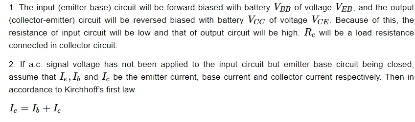
It explains diodes, transistors, and logic gates, highlighting their roles in switching, amplification, and rectification. The chapter also introduces communication systems, including signal transmission and reception, modulation techniques like AM and FM, bandwidth requirements, and modern telecommunication tools such as satellites and optical fibre transmission, emphasizing their relevance in today’s networks.
These notes provide students with a concise and clear revision guide, ideal for last-minute preparation before the 2026 board exam.
CBSE Class 12 Physics Notes Chapter 14 Overview
Semiconductor Devices and Communication Systems, Chapter 14 of CBSE Class 12 Physics, examines the basic ideas behind semiconductors and how they are used in contemporary electronics and communication. The first section discusses materials with conductivity qualities that fall between those of conductors and insulators, such as silicon and germanium. Introduction to important semiconductor devices: p-n junction diodes, Zener diodes, and transistors; their uses in switching, amplification, and rectification circuits are explained.CBSE Class 12 Physics Notes Chapter 14 PDF
Below we have provided CBSE Class 12 Physics Notes Chapter 14 Semiconductor Devices & Communication System pdf for the students, so that they can download it and access it offline.CBSE Class 12 Physics Notes Chapter 14 PDF
CBSE Class 12 Physics Notes Chapter 14 Semiconductor Devices & Communication System
Below we have provided CBSE Class 12 Physics Notes Chapter 14 Semiconductor Devices & Communication System - Solids have single energy levels where the atoms are arranged in a systematic space lattice. As a result, for an isolated single atom, the neighbouring atoms have a significant influence on the atom.Insulators
In the case of insulators, the forbidden energy band will be extremely broad. This knowledge prevents electrons from jumping from the valence band to the conduction band. In insulators, the valence electrons will have an extremely strong link with their parent atoms. Certain electrons will be able to migrate to the conduction band when the temperature rises.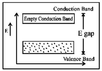
Semiconductors
In semiconductors, the prohibited band will be quite narrow. You can use silicon and germanium as examples of semiconductors. Any material with electrical properties that fall between those of an insulator and a good conductor is considered a semiconductor. The electrons can move with ease from the valence band to the conduction band if only a small amount of energy is applied. For instance, an increase in temperature will cause the forbidden band to shrink and some electrons to be released into the conduction band.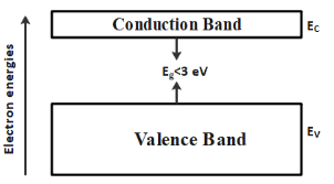
Conductors
In the case of conductors, there won't be any prohibited bands, and the valence and conduction bands will overlap. Here, there will be a large number of free electrons available for the conduction of electricity. The free electrons that cause the electric current will be caused by a tiny potential difference across the conductor. The important thing to remember about conductors is that without a restricted band, there wouldn't be a framework for creating holes. All that remains of the current in conductors is only an electron flow.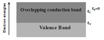
Semiconductors
Therefore, a material exhibiting resistivity between conductors and insulators can be referred to as a semiconductor. The characteristics listed below will be present in semiconductors. (i) They'll be more resistive than conductors and less than insulators. (ii) A semiconductor's resistance will decrease when temperature rises and vice versa. (iii) A semiconductor's current conducting properties vary noticeably when an appropriate metallic impurity, such as arsenic, gallium, etc., is added. Impact of temperature of Semiconductors: Because there are no available free electrons and the covalent bonds are essentially strong, the semiconductor crystal will function as a suitable insulator. The thermal energy imparted to the crystal at normal temperature will cause some of the covalent bonds to break. Some of the electrons that were inhabited during the formation of these bonds will become free as a result of the bonds breaking. A little circle can be used to symbolise the covalent bond's electron's non-appearance. As a result, Hole can be understood as a gap or empty space that remains in the crystal structure. A hole will likewise have a unit positive charge since an electron has a unit negative charge.Pure or Intrinsic Semiconductor and Impure or Extrinsic Semiconductors
A semiconductor that produces its electrons and holes only through thermal excitation is known as an intrinsic semiconductor. Alternatively, a pure semiconductor is referred to as an intrinsic semiconductor. In an intrinsic semiconductor, the number of free electrons is always equal to the number of holes.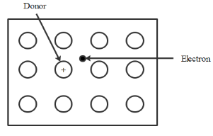 A pure semiconductor crystal can be transformed into an N-type extrinsic semiconductor by adding a little quantity of pentavalent impurity during the crystal's development. The following things to keep in mind when using N-type semiconductors (i) In an N-type semiconductor, electrons will constitute the majority carrier and positive holes the minority carrier. (ii) N-type semiconductors are electrically neutral despite having an excess of electrons. This is due to the fact that when neutral pentavalent impurity atoms are added to the semiconductor, electrons are created. In other words, neither positive nor negative charges will be added.
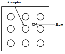 If a little amount of trivalent impurity has been added to a pure crystal while the crystal growth, the produced crystal can be referred as P-type extrinsic semiconductor. When considering P-type semiconductors, keep in mind the following: (i) In P-type semiconductor materials, electrons are the minority carrier whereas positive holes are the majority carriers. (ii) The P-type semiconductor will continue to be electrically neutral as long as there are always the same number of mobile holes relative to acceptors.
P–N Junction Diode
A P-N junction is formed when two P-type materials are tightly connected. Since the surface coatings and other defects create a significant discontinuity in the crystal structure, joining the two pieces will not result in the formation of a P-N junction. Therefore, by diffusing P-type material to one half side and N-type material to the other half side, a P-N junction will be formed from a piece of semiconductor, such as germanium. An assembly known as a P-N junction diode is needed if two P-type and N-type crystals are kept in contact to form a single component.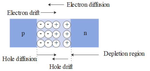 Forward Bias If an external direct current source is connected to the junction diode, with the p-section linked to the positive pole and the n-section to the negative pole, the diode can be classified as forward biassed.
 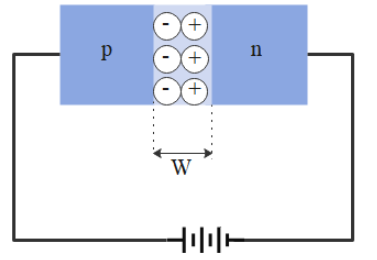 Reverse Bias If an external DC battery is connected to the junction diode with the P-section linked to the negative pole and the N-section connected to the positive pole, the junction diode is said to be reverse biassed.
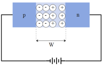
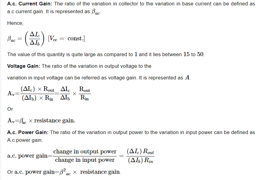
Common Emitter Amplifier:
Amplifier Circuit by the Use of n–p-n Transistor
Common Base Amplifier
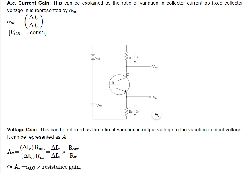
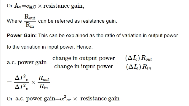
Common Emitter Amplifier
Universal Gate
A logic gate that may be utilised to carry out any Boolean function without the need for any other kind of logic gate is known as a universal gate. The NOR and NAND gates are two types of universal gates.Integrated Circuits
The traditional method of building circuits involves selecting parts such transistors, diodes, R, L, C, and so on, then soldering wires to connect them in the necessary ways. The Monolithic Integrated Circuit will be the most widely used technology. Logic gates are a component of these circuit types.Benefits of CBSE Class 12 Physics Notes Chapter 14
For students getting ready for their board exams, the CBSE Class 12 Physics notes for Chapter 14, "Semiconductor Devices and Communication Systems," are quite helpful. This is how they can assist: 1. Concise and Focused Study Material CBSE Class 12 Physics Notes Chapter 14 summarize the vast syllabus into key points, making it easier to grasp the essential concepts. Important formulas, definitions, and diagrams are highlighted for quick revision.CBSE Class 12 Physics Notes Chapter 14 FAQs
Is semiconductor class 12 difficult?
Is pn junction the key to all semiconductor devices?
Is semiconductor a big chapter?
What is the formula for semiconductor chapter?
What is the symbol of pn junction?